|
|
Have Sample, Will Travel
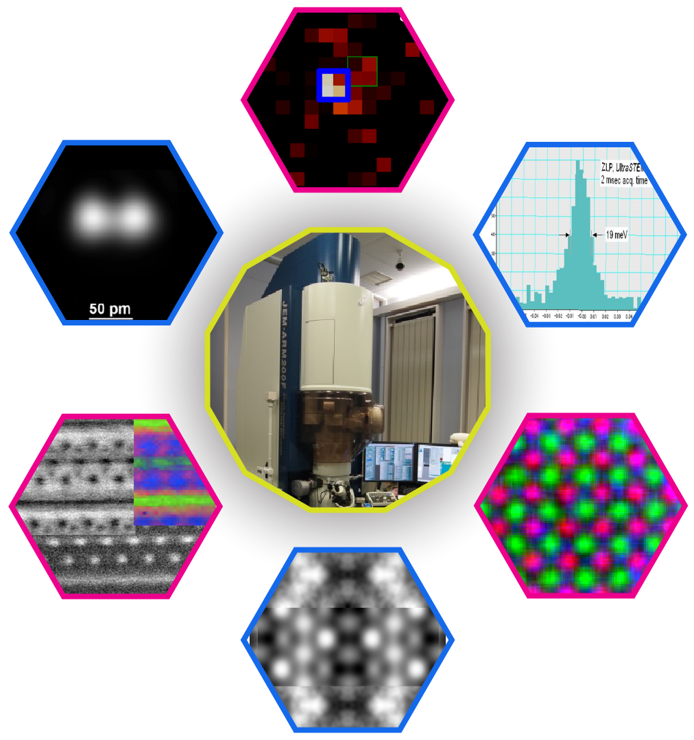 The improvements in electron microscopy in the last decade have been amazing. As illustrated on the left, images from single atoms have been obtained; electron energy
loss spectroscopy is approaching 10 meV where phonons can be imaged, EDS in commercial instruments has atomic resolution,
SEM images of monolayer surface reconstructions has been achieved, multiple structural and imaging modes are available simultaneously and 50pm resolution is
now achievable, Indeed, electron microscopy has left behind use of "nanometers" and "picometers" has become the norm to describe resolution.
The improvements in electron microscopy in the last decade have been amazing. As illustrated on the left, images from single atoms have been obtained; electron energy
loss spectroscopy is approaching 10 meV where phonons can be imaged, EDS in commercial instruments has atomic resolution,
SEM images of monolayer surface reconstructions has been achieved, multiple structural and imaging modes are available simultaneously and 50pm resolution is
now achievable, Indeed, electron microscopy has left behind use of "nanometers" and "picometers" has become the norm to describe resolution.
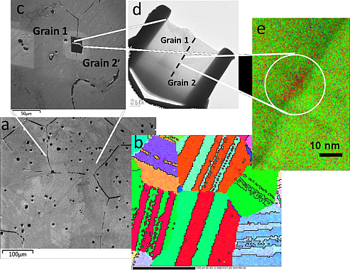 Using conventional instruments one can obtain extensive information across the size scales, for instance on carbide
precipitates at grain boundaries that corrode in CoCrMo alloys used for orthopedic implants, as shown in the Figure
on the right. One can do much more with bleeding-edge electron microscopes.
However, the price to purchase and maintain the hardware has risen with the improvements, so now no single university or indeed National Laboratory
can hope to have a complete range of instruments. A key concept in our research plan is "Have Sample, Will Travel" as well as use of other national
or international facilities. This has dominated the x-ray synchrotron and modelling communities for years, and is a recent innovation in the electron
microscopy community. With the exception of the unique UHV instrument at Northwestern, we intend to exploit aberration-corrected and other
specialized instruments around the US and in some cases internationally via the existing collaborative networks of the PIs.
Using conventional instruments one can obtain extensive information across the size scales, for instance on carbide
precipitates at grain boundaries that corrode in CoCrMo alloys used for orthopedic implants, as shown in the Figure
on the right. One can do much more with bleeding-edge electron microscopes.
However, the price to purchase and maintain the hardware has risen with the improvements, so now no single university or indeed National Laboratory
can hope to have a complete range of instruments. A key concept in our research plan is "Have Sample, Will Travel" as well as use of other national
or international facilities. This has dominated the x-ray synchrotron and modelling communities for years, and is a recent innovation in the electron
microscopy community. With the exception of the unique UHV instrument at Northwestern, we intend to exploit aberration-corrected and other
specialized instruments around the US and in some cases internationally via the existing collaborative networks of the PIs.
|